
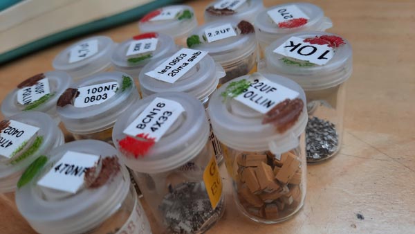
So everthing is here what I need to build up... So let's get started.
I've decided to solder the lower part of the PCB first. Well after soldering the FPGA I do not want to heat up the entire stuff in the reflow oven. Not that the soldered FPGA fall off... Dunno I have no experience here anyway...
But soldering the lower side first then the upper side i'm pretty sure the surface tension will keep the components on the lower side in place.
So stencil foil is placed and not let's print the soldering paste to the PCB:
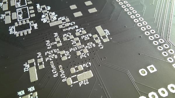
Printing went well even the smaller components got some solder... The small 0,47uf components are 0402 (1mm x 0.5mm) parts. A pain in the pass to place by hand. One tip do not drink too much coffee before placing.;)
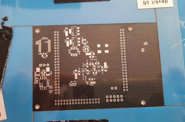
This stuff (ok only parts of it) needs to be placed.
Here:
Placement of the important componets is done. Reflow time...

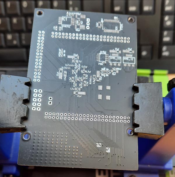
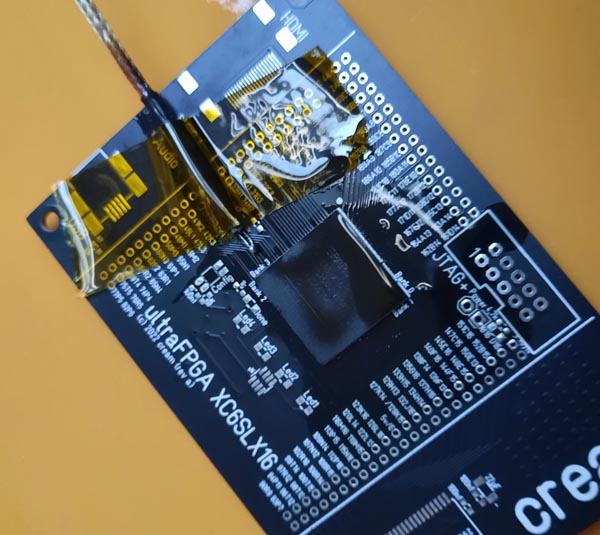
Reflow looks pretty good. I only added the needed components for the project i'm working on currently usb, audio and ram is not soldered in.

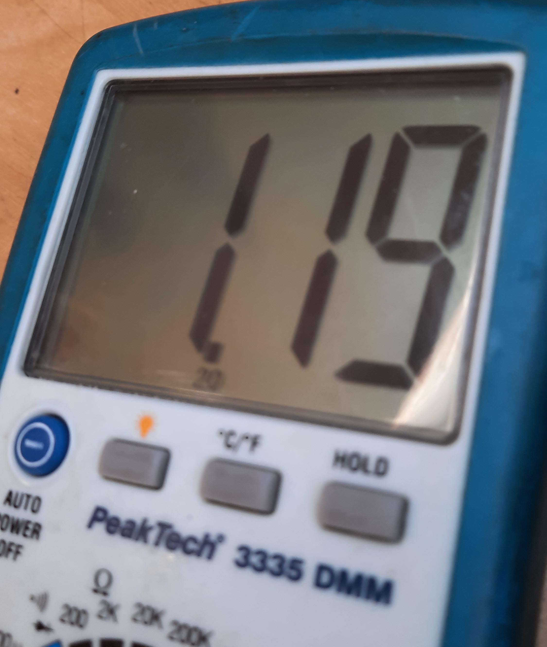
The lower side is mainly providing the power for the PCB. So let's check the power rails.
About 1.2v and 3.3v is all we need.
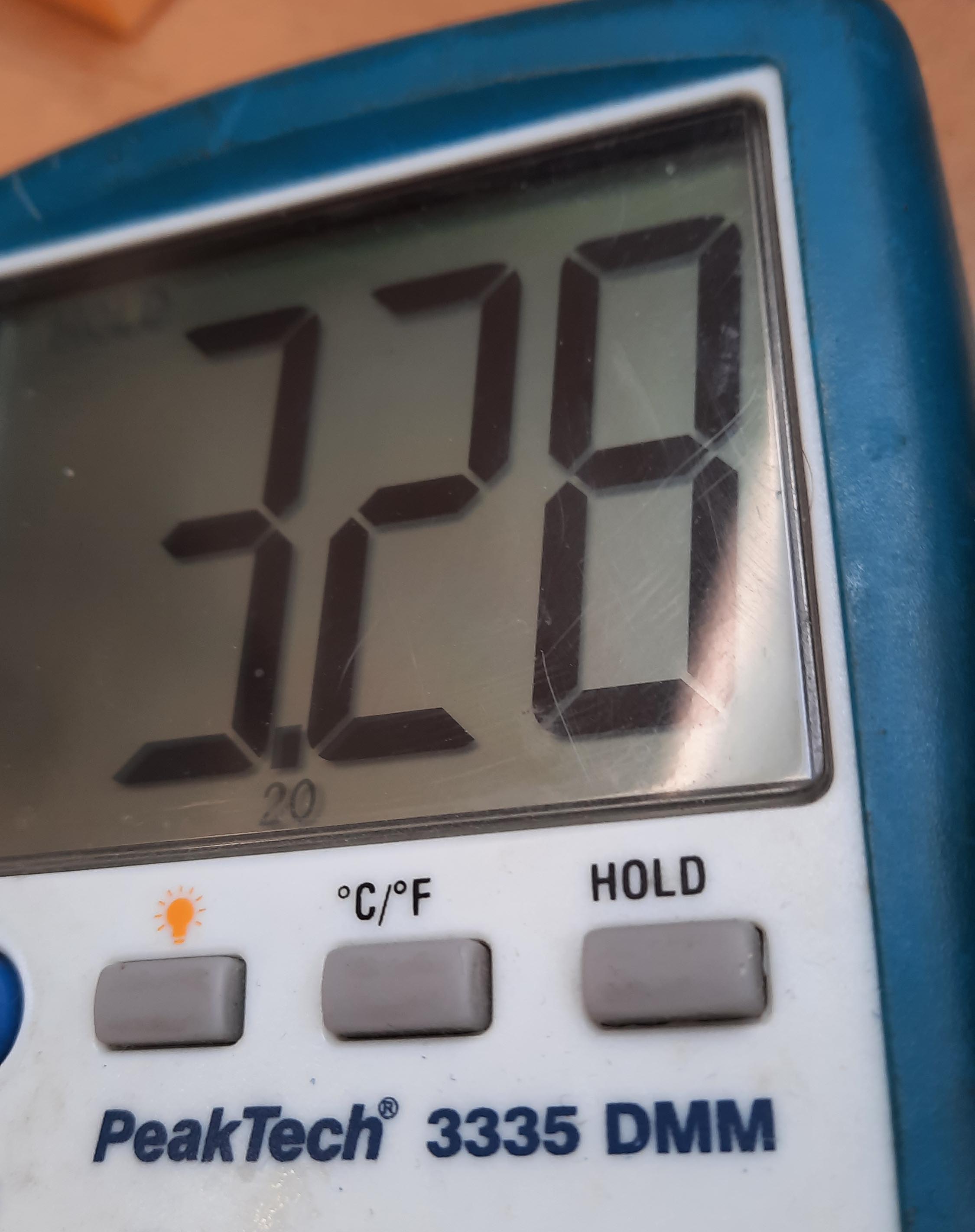
For using the FPGA you need a clock. Otherwise nothing works. I added a 80mhz oscillator to the board. Let's check that first.
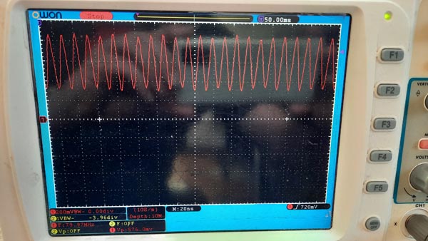
On the lower left you can see the 79,97Mhz. Ok looks good. So power rails and oscillator are working fine.
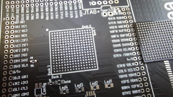
Next up is to solder in the FPGA. That's the most challenging part.
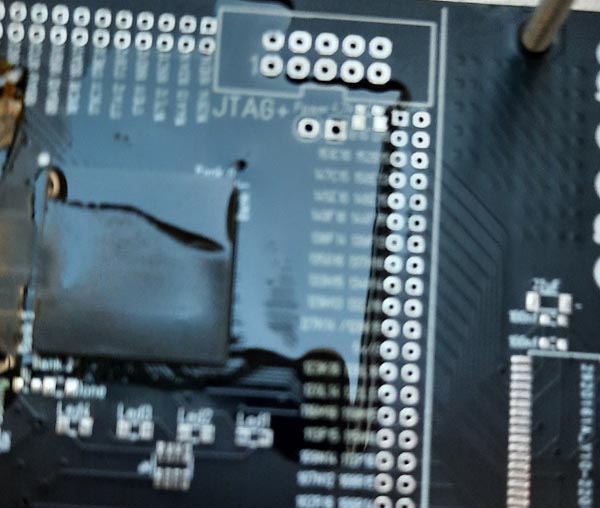
For this I added flux to the area and added alot of soldering tin to the pads. Just to be sure the pads do not have leaded tin on it. This will drop down the melting point of the solder.
Next to remove the solder again with solder wick flux. I used hot air to preheat the area and scraped thru the area (carefully) with the solder wick and solder iron to remove all tin.
Why I do use the hot air gun here? Well this will give a better temprature and will avoid of killing some pads. Result looks like this:
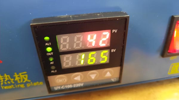
The PCB shortly before soldering. In the back you can see the heating plate to heat up the entire PCB from the lower side. That thing on the left is a thermocouple to measure the temperature of the PCB on the upper side.
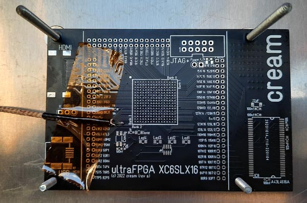
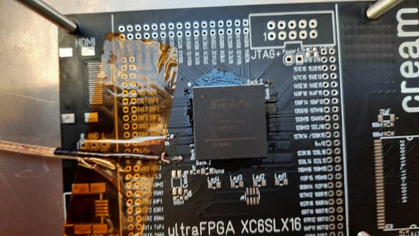
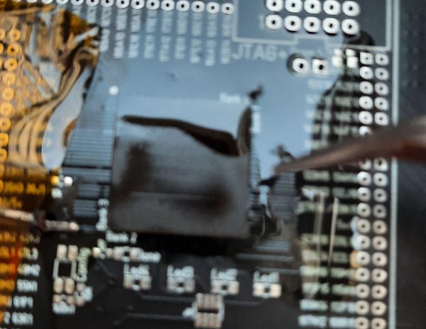
Placement of the FPGA is done. Of course i added some flux...
Time to heat up the plate. Ahhh well... now I'm getting reaaaaaaaally nervous. Doing this for the first time.
After some time I added some more flux to ensure all stuff is soldered fine under the FPGA. Ok that's maybe a bit too much... anyway too late to change ;)
After some time I started heat up the upper with hot air. When the soldering temperature is reached i wait a while (small). Then I gave the FPGA a mini kick from the side. If solder melted it will snap back into the right position That's a good check to see if you can stop heating up. But i gave it some more time to solder just to be sure.
When the PCB dopped down to about 90�c I removed it from the heating plate (took a while till 90�c):
And another slow cool down... 51�c looks good now I can continue...

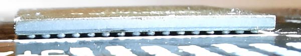
Soldering looks good so far i can judge ;) Well first BGA soldering
In the end i measure all IO pins with a multimeter against GND in diode mode. All pin showed a result of 0,3xx or so means there is a connection from the FPGA to the PCB.
Before powering up last check if there is a short cut between 1.2v to GND and 3.3v to GND. Nope Looks good
First power up and connecting the FPGA to the Xilinx programmer.
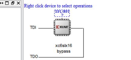
Holy shit. The FPGA is recognise by the Xilinx programmer. That is awesome...
Time to fire up the IDE and do a small test programm.
And what is the first you always try? Excatly to try to let some leds blink.
WORKS !
That what I call a successful build up. ;) Ok I did not check if the FPGA boots up but tbh I don't care I can upload stuff and do some things on Spartan 6 ;)
Round up of the first usage of BGA chips.
Doing the PCB with a 4 layer PCB is really no big deal. Fan out of the pins with my package was no real problem.
Placing and soldering the FPGA was also not very hard (ok used a 1mm pitch package anyway). Doing that at home with semi professional equipment is no big deal.
Only the heating plate is not that good i bought... It has too less power. Heating up takes ages but anyway maybe better for the FPGA ;)
Using the silk screen to do marks to place the FPGA is maybe not that a good idea... I recognised the silk screen marks are slightly off from the copper. I have to change that in the next BGA PCB... Ok should be clear that it can be a bit off but anyway didn't thought of that but luckily it was no problem...
In the end I regret not doing this alot earlier. I always avoided BGA packages until now because I had too much respect to create the PCB and finally the soldering.
Well before i was bound to a really old IDE version of Xilinx which still supports the Spartan 3. Means I can finally use the new Vidado of Xilinx... Yay...